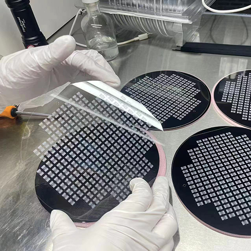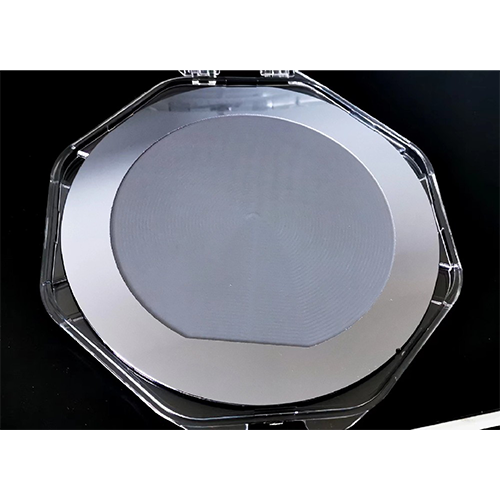

TGV Substrate
The advantages of through glass via (TGV) and through silicon via (TSV) compared to TGV are mainly reflected in:
1) Excellent high-frequency electrical characteristics. Glass material is an insulator material, the dielectric constant is only about 1/3 of that of silicon material, and the loss factor is 2-3 orders of magnitude lower than that of silicon material, which greatly reduces substrate loss and parasitic effects and ensures the integrity of transmitted signals ;
2) Large-scale ultra-thin glass substrates are easy to obtain. Glass manufacturers such as Corning, Asahi, and SCHOTT can provide ultra-large (>2m × 2m) and ultra-thin (<50µm) panel glass and ultra-thin flexible glass materials.
3) Low cost. Benefiting from the easy availability of large-size ultra-thin panel glass and the need not to deposit an insulating layer, the manufacturing cost of a glass interposer is only about 1/8 of that of a silicon-based interposer;
4) The process flow is simple. There is no need to deposit an insulating layer on the surface of the substrate and the inner wall of the TGV, and no thinning is required in the ultra-thin interposer;
5) Strong mechanical stability. Even when the interposer thickness is less than 100µm, the warpage is still small;
6) It has a wide range of applications. It is an emerging vertical interconnection technology applied in the field of wafer-level packaging. It provides a new technical approach for realizing the interconnection with the shortest distance between chips and the smallest spacing. It has excellent electrical, Thermal and mechanical properties have unique advantages in the fields of RF chips, high-end MEMS sensors, and high-density system integration. It is one of the first choices for 3D packaging of next-generation 5G and 6G high-frequency chips.