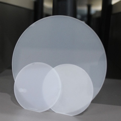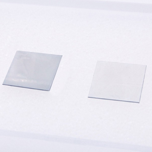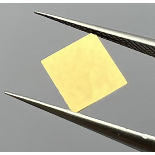

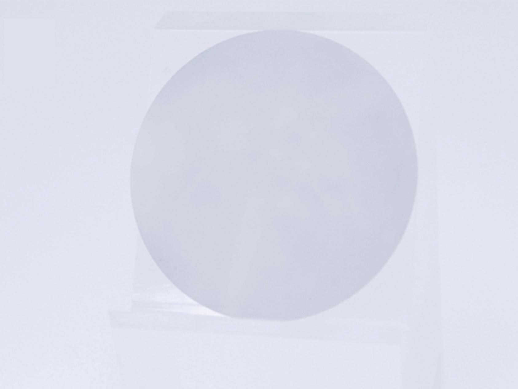
CVD DIAMOND WAFER
Single crystal and polycrystalline diamond
High-quality diamond grown by the MPCVD method, supplemented by an efficient and precise processing method of original plasma polishing, achieves a surface roughness of wafer-level diamond growth surface Ra<1nm (5*5um), or even lower than 0.5nm, reaching an internationally leading level level
A.
Size: 10*10mm, 5*5mm, etc.
Thickness: 0.2-1mm, etc., can be customized
B.
Thermal conductivity:1000-2200W/(m·K)
C.
Surface roughness Ra<1nm (5*5um),
Back Ra<20nm, can be customized
D.
Wafer warpage <300um, can be customized
| Tyep | Single Crystal Diamond | Polycrystalline diamond |
| Thermal conductivity | >2000W/(m·k) | 1000-2200 W/(m·k) |
| Surface roughness | Ra<1nm | Ra<1nm |
| TTV | / | <30um(2inch) |
| Warpage | / | <300um (2inch),customizable |
| Flatness PV | / | <15fringe(020mm) |
*The above are standard product specifications, and customized services can be provided according to customer requirements.
Testing Data--Surface Roughness
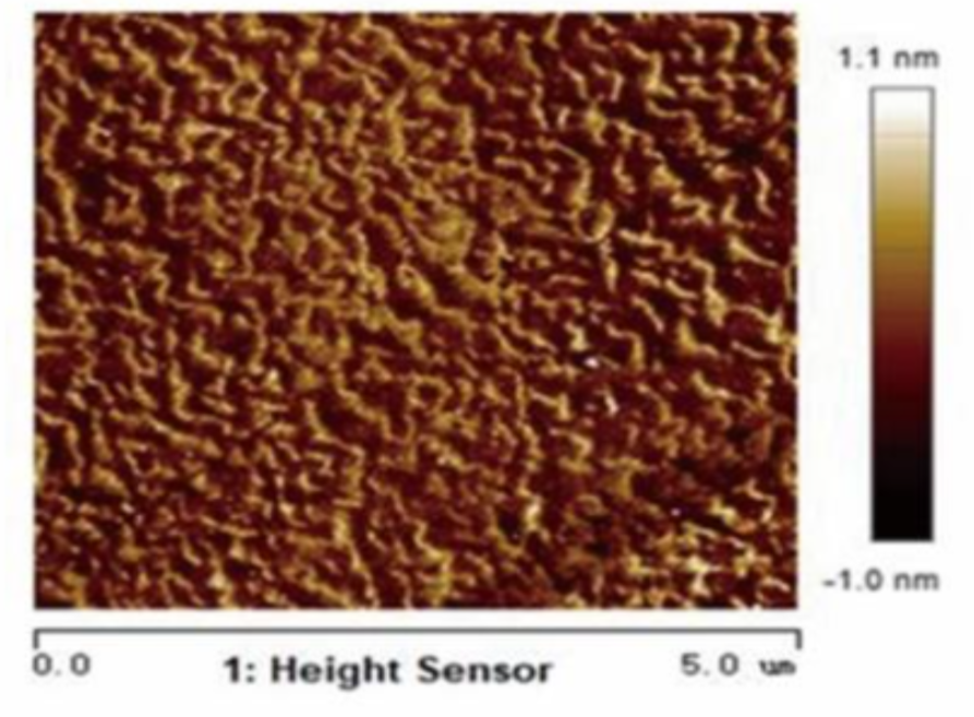
FIG1:Ra=0.278nm
Testing Data--Thermal conductivity
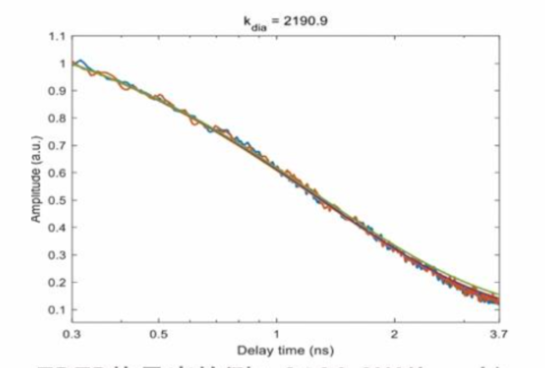
FIG2:Thermal conductivity detection: 2190.9W/(m·k)
Testing Data--Wafer Warpage
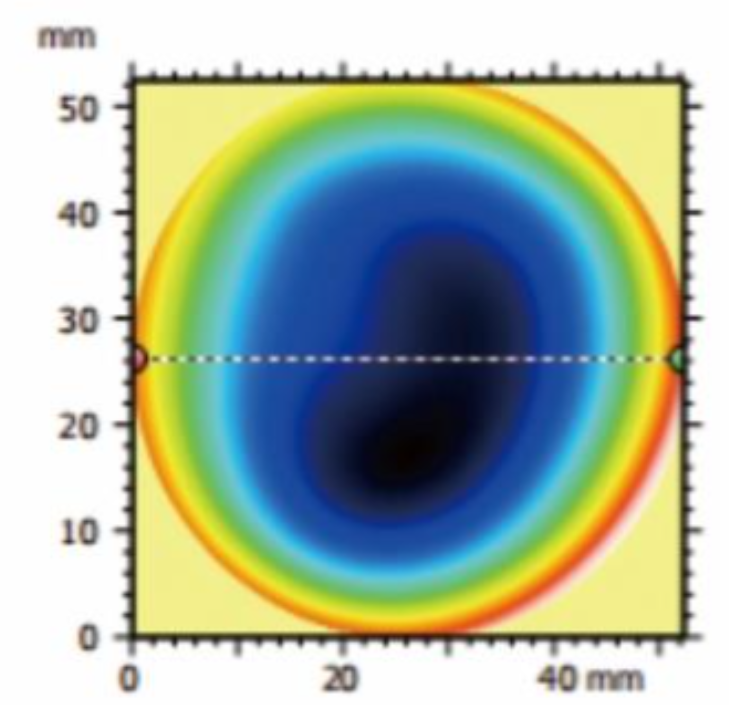
FIG3:Warp:43.856um
More Application:
Optical Window
A.diamond material X-ray windows
B.diamond material High Power laser optical window,such as CO2 Laser ,disk laser
C.diamond material high power laser multispectral optical window
D. diamond material High-power millimeter-wave windows
Thermal Management
A.diamond material heat sink/submount
Semiconductor
A.diamond wafer
B.GaN on diamond